Our most recent paper, which was published in Energies, looks at the optimisation of scribes for fully printable carbon perovskite solar modules in order to improve efficiencies. Here, lead author Dr Simone Meroni discusses the processes and research that led to the paper being published.
Making solar modules is not like making single solar cells. When working on single cells, the main parameters that should be optimised include the power conversion efficiency (PCE) of the device and the cost of the materials. When making modules, an additional parameter must be considered: the geometric fill factor (g-FF).
The g-FF is a number that tells us how much the active area covers the total area of the device. Let’s consider two devices with different PCE, for example: 20% for the first and 15% for the second. Obviously, the first device behaves much better than the second. However, if the relative modules have a g-FF of only 20% for the first device and 80% for the second device, the power conversion relative to the total area of the device is 20% x 30% (= 6%) in the first module and 15% x 80% (= 12%) in the second module. This means that for the same device size, the second module generates much more power than the first one, despite the higher PCE per active area unit!
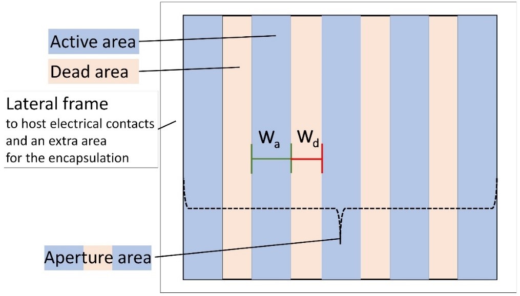
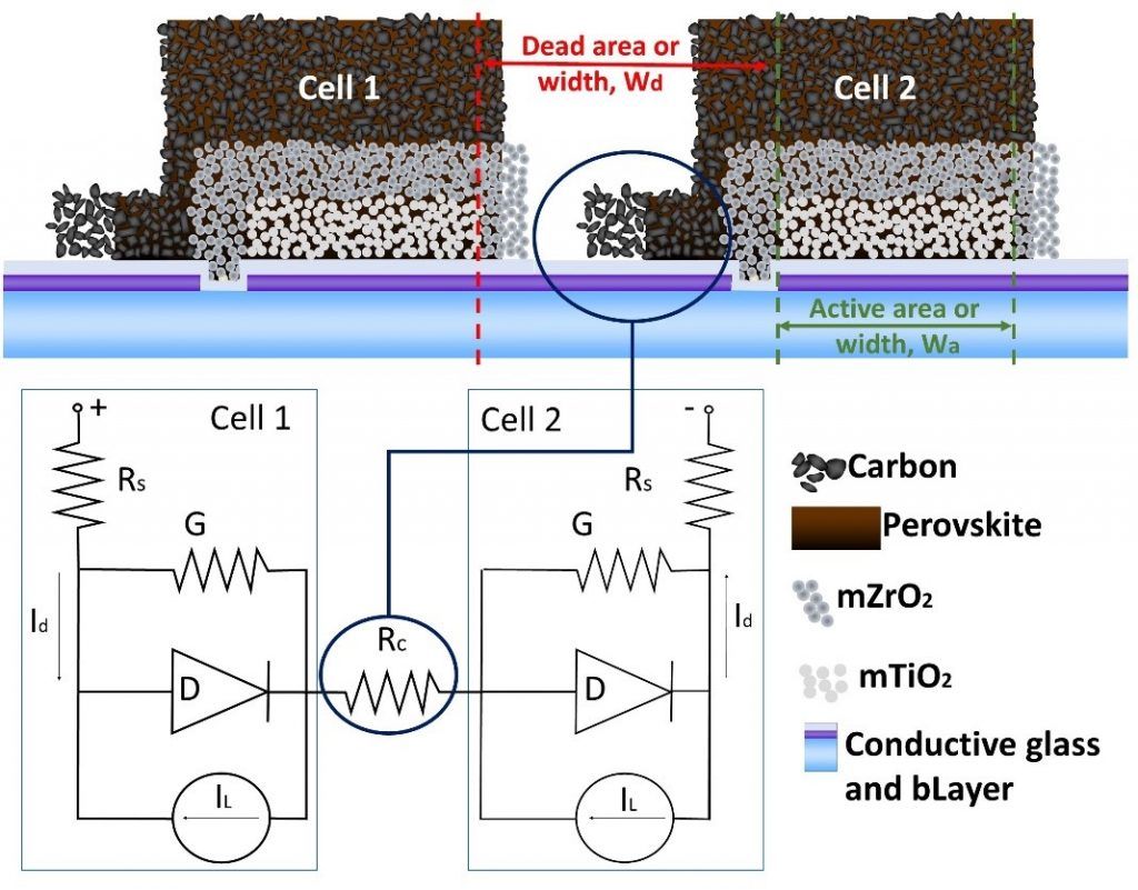
The g-FF is a key parameter when designing large area modules. The main obstacle when achieving high g-FF is the distance between the single cells. The distance between the cells is a dead (inactive) area but is useful as it hosts the interconnects. The interconnects are key to overcome the limit of low conductivity of transparent electrodes, and they occupy a space. The dead area, therefore, can be minimised according to the accuracy of the layer patterning and the space that is occupied by the interconnects.
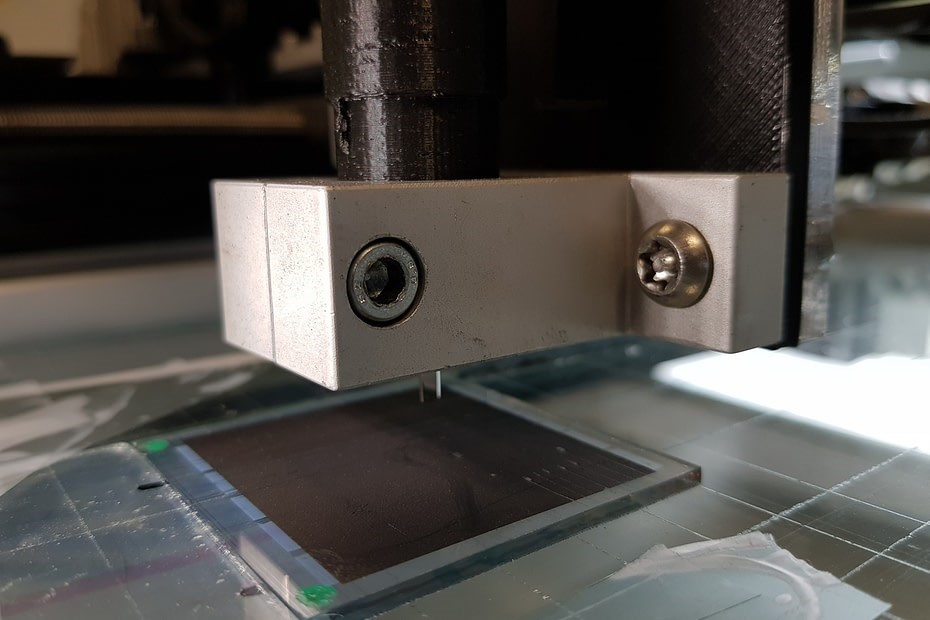
The scribing method involves the deposition of layers on a solid large area, and then the removal of a tiny amount of material. This is to properly scribe and create the interconnects. The method allows g-FF above 90%, as already proven with many solar cell architectures.
So, how can this method be applied for the fully printable carbon perovskite solar cell (C-PSC)? And why does this matter?
The C-PSC is a very promising technology for future applications. It is a candidate to achieve market penetration in the near future due to:
- the high stability of a perovskite solar cell (over 1 year under constant illumination)
- the low cost of the material (no noble metals as top contact or other expensive organic materials)
- the low cost of the fabrication process (based on the industrial established screen-printing method)
- the low-capital cost
Modules based on C-PSC have been fabricated via registration. In this method, the interconnects are created via accurate registration of each layer. The accuracy of the method depends on the quality of the printer (and equipment costs). The distance between two stripes in the same printed layer can be less than 1mm when the process and the ink formulation are properly optimised. The scribing method allows scribes of less than 50µm via laser scribing (especially with pico or femto-second lasers) or less than 200µm via mechanical scribing.
It’s evident that the scribing approach allows higher g-FF. However, high accuracy is not enough to minimise the distance between cells, because the contact area must be minimised as well. If the distance between the cell is too short, there is not enough contact area to properly allow the charge collection. The porous carbon layer that is used as a top electrode in the C-PSC is not as conductive as compact metal layers. For a metallic top electrode, the contact area is usually between 100 and 200 µm. How wide should a contact with a porous carbon electrode be?
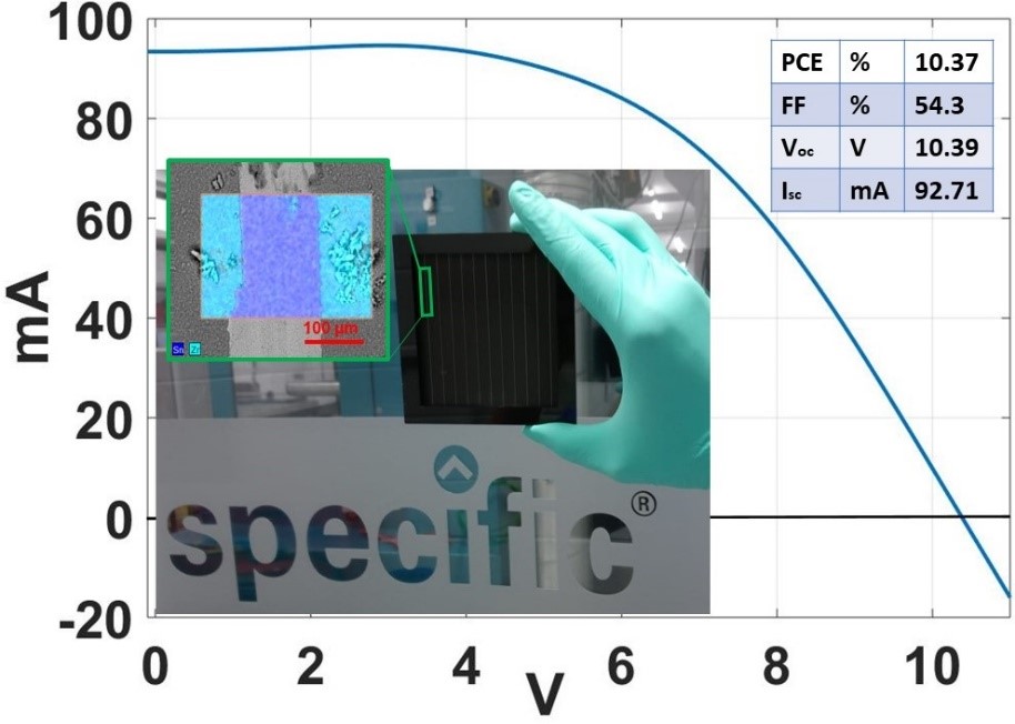
In this work, we show the effect of the contact area on the module design and the effect of the distance between the cells. This work was carried out on 5 x 5cm mini-modules and then scaled-up to 10 x 10cm. The same approach was then used to make much larger modules.
I’m so happy that my work on the scribing method to fabricate fully printable solar modules is available in an open access journal, Energies. I thank the SUNRISE and SPECIFIC teams for the support.