Cheaper, lighter, more efficient: there are lots of promises associated with the next-generation of photovoltaics (PV). But what is the next generation of PV? And will it live up to the hype?
What are next-generation photovoltaics?
The definition of ‘next-generation photovoltaics’ is a tricky one to pin down. Crystalline silicon PV is considered first-generation, which currently dominates market production. Thin-film technologies that use less material, such as cadmium telluride (CdTe) and copper indium gallium selenide (CIGS), are classed as second generation. These constitute about 6% of the global market. Next-generation PV comprises a range of new materials and designs such as organic and perovskite PV, some of which are now being scaled “from lab to fab.”
A notable characteristic of the different generations of PV is the manufacturing process. A mature technology like silicon has a limited number of distinct manufacturing methods followed by numerous companies. This means that process breakthroughs can be adopted rapidly and have a big impact. Next-generation technologies, however, are yet to develop standard manufacturing approaches or architectures and the characteristics of one design may not transfer to others.
Sam Stranks, Professor of Optoelectronics at Cambridge University said:
“I consider next-generation solar to be technologies with efficiencies beyond current state of the art (particularly tandems to push modules to 30%), and new manufacturing paradigms that could potentially allow more local, modular manufacturing – mitigating future supply chain risks and manufacturing geopolitics, and opening opportunities for local job creation and technological expertise.”
Whereas Professor Jenny Nelson from Imperial College London responded:
“To your question of what constitutes next generation solar, I would think of systems designs and integration approaches that minimise the costs so that solar electricity is affordable and available. I think we need that whatever the semiconductor is.”
Why do we need next-generation PV?
The scale-up of silicon PV manufacturing over the last 15 years has transformed electricity generation in many parts of the world. But the modules have largely not been designed with end-of-life considerations in mind. With a continued growth in demand we face the prospect of vast amounts of waste, unreclaimed materials and environmental consequences. Thin film PV technologies, whilst they offer some attractive characteristics, use a number of critical raw materials that may limit their contribution to the energy transition.
Next-generation PV technologies at a pre-commercialisation stage, such as perovskites, have a significant opportunity to be designed with their full life-cycle in mind. As such, they would be fully recyclable at the end of their lifetime. They can encompass the best characteristics of both silicon and thin-film technologies in terms of efficiency and materials usage yet be made using low-cost, earth-abundant elements.
Further elements of next-generation PV include:
- Cheaper and simpler to manufacture using lower temperatures
- Lighter (making them suitable for applications such as building-integrated PV and space)
- Can perform better at higher temperatures
- Perform better in low light
What are the challenges facing next-generation photovoltaics?
As with any technology in the early stages of development, there are challenges to overcome. Primarily, we need to improve the efficiency and stability of next-generation PV modules. To be commercially viable, they must demonstrate sufficient lifetimes and power outputs to justify the carbon and financial cost of producing them. If they cost more money or produce more emissions than they would save in their lifetime, then they are not an effective technology.
Scaling-up next-generation PV is a particular challenge. The lab-based processes used to make high-performing devices often don’t work at scale. Therefore, you can’t just make the lab equipment bigger – in many cases you need to apply an entirely different process when fabricating the modules at scale.
Supply chains and materials availability are also potential obstacles. Some of the chemicals required to make next-generation PV are not currently manufactured at scale. And many perovskite devices incorporate materials like Caesium, Indium, and Gold, which are not readily available. Hypothetically, to produce a Terawatt-scale output from next-generation PV using these materials, you would need a projected production increase of over 1000% in some cases.
How are we supporting the development of next-generation PV?
At SPECIFIC, we specialise in developing the pathway from small, lab-scale devices right through to large-scale integration into buildings. Our research teams are developing technologies and techniques that will allow high-efficiency, printed photovoltaics to be manufactured at scale using earth-abundant, low-cost materials. But we don’t work in isolation. We collaborate with both academia and industry to bridge the gap.
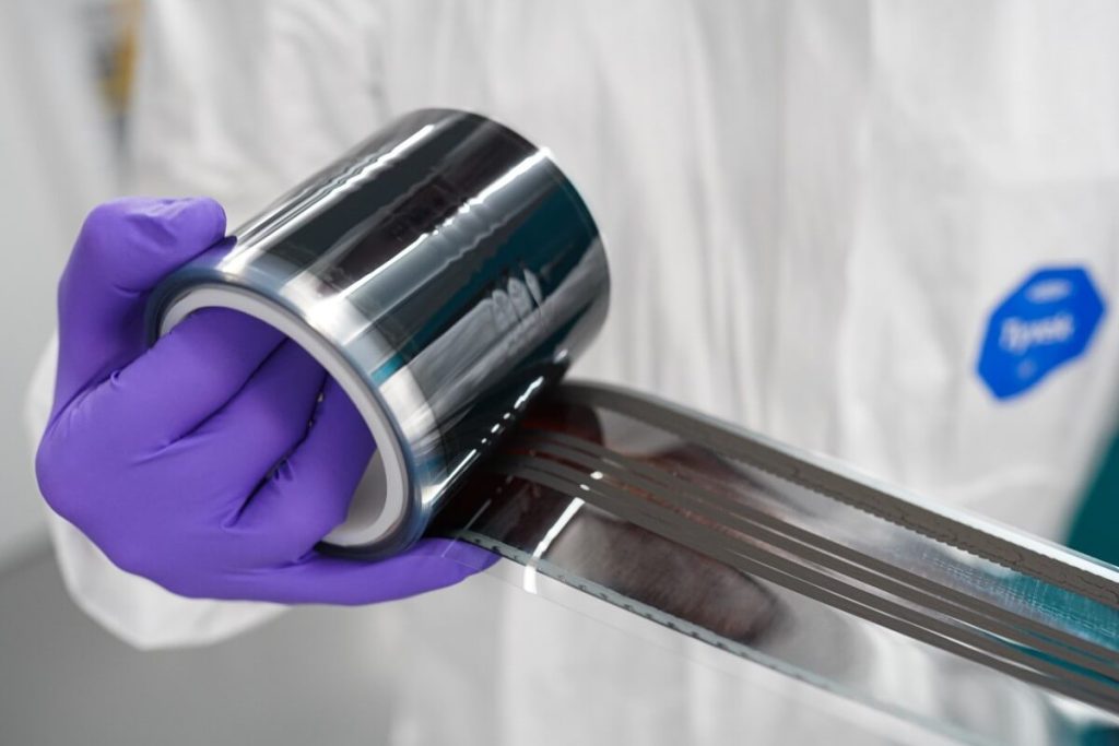
We recently developed the first fully roll-to-roll printed perovskite solar cell, which uses a low-cost and scalable carbon ink formulation to replace the gold electrode. Our new formulation makes high-volume manufacturing easier and more economical. As such, it is a big step towards the commercialisation of perovskite solar cells. A unique collaborative team of chemists, materials scientists, and engineers made this research possible.
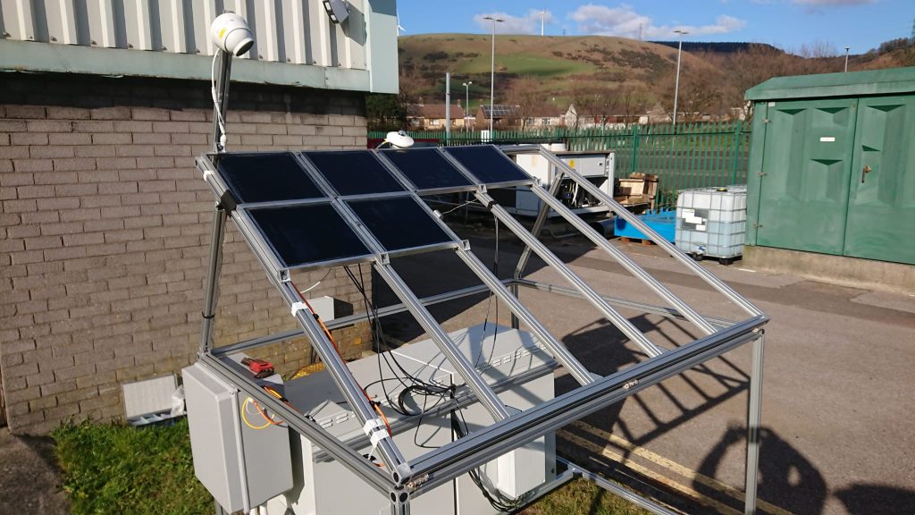
We are also developing large-area glass encapsulated modules. We have been testing the first UK-made carbon perovskite solar panels on two weathering stations. One is at our SHED (Solar Heat Energy Demonstrator) in Baglan and the other on the campus of our partners in Mexico – CINVESTAV University Merida. Our researchers designed these 30 x 30cm panels using techniques that are easily scaled-up, including screen-printing, drop casting and mechanical scribing. The team is working with CINVESTAV to improve the performance and stability of these devices.
At the other end of the spectrum, we also work with companies to help them develop new technologies and accelerate the uptake of next-generation PV. We recently collaborated with A&B Smart Materials to support them with a materials assessment of their novel, smart hydrogel. This hydrogel could be used for cooling solar panels, improving efficiencies and power outputs.
Next-generation photovoltaics for a just transition
Finally, we need to make sure this technology can promote a sustainable and equitable energy transition. A new project, TEA at SUNRISE, will support the local manufacturing of next-generation PV in countries in Africa, Asia, and the Indo-Pacific.
As we have previously mentioned, silicon PV has not been designed to be fully recycled. But neither is its manufacturing globally distributed. By accelerating the scale of locally-manufactured, sustainable, next-generation PV in these regions, the project hopes to create local jobs, boost the economy, and reduce the environmental impact of PV production.
Led by Swansea University and building on the pre-existing SUNRISE network, the project will form an interdisciplinary and international collaboration across the UK, Africa, Asia, and Indo-Pacific. This network will identify and deliver on local opportunities for next-generation photovoltaics.
Thank you to Dr Mark Spratt and Dr Carys Worsley for their contributions to this blog post.